
Via in Pad Lead to Weak Pads
While vias in pads make for easier routing of high-frequency signals, they come with their own set of challenges that designers should be aware of. Among them are the risk of solder voiding and increased manufacturing complexity and cost. The good news is that these issues can be managed if careful design practices are followed.
One of the common myths about via in pad is that it weakens the pads, making them more likely to detach from the PCB after repeated cycles or high temperatures. While this may sound true, the truth is that a via in pad actually strengthens the SMD pads by providing anchoring into an internal conductor. This allows the pad to better resist thermal expansion and mechanical stress.
In addition to strengthening the SMD pads, via-in-pad can improve board thermal performance by reducing convective heat. This is particularly important in high-speed and high-frequency designs, where signal integrity must be maintained and temperature gradients must be minimized.
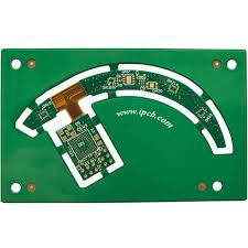
Does a Via in Pad Lead to Weak Pads?
Via-in-pad can also simplify routing by eliminating the need to route signal nets over traditional fan outs. This enables shorter paths to power and ground planes that can help reduce parasitic inductance and EMF emissions. This can also simplify BGA and LGA device footprints, allowing designers to utilize the space underneath devices to maximize package density.
Another reason for the popularity of via in pad is that it can allow designers to reduce component footprint size by placing vias directly in component pads. This is especially important for fine-pitch BGAs, where there is often not enough room to fit dog bone fanouts underneath the package without violating clearance requirements.
When used correctly, via-in-pad can significantly increase the reliability of a circuit board by preventing solder voiding during the reflow process. Voids can lead to a loss of electrical continuity and weaken the mechanical strength of the solder joint, which can be an issue in critical applications such as aerospace or medical devices.
By using resin or electroplated fills, designers can minimize the likelihood of voiding during reflow. Resin fills use non-conductive materials like epoxy to fill the via, which prevents solder wicking and provides mechanical stability. Conductive epoxy can also be used, if needed, to ensure electrical continuity and help dissipate heat.
Using the right type of fill can also help ensure that a via is not exposed to the elements in the environment in which the board will be used, as this can increase its longevity. The choice of which type of fill to use depends on the requirements of the particular application and the manufacturer’s capabilities.
To avoid potential problems with via-in-pad, it’s critical to run detailed design for manufacturability (DFM) checks. This includes reviewing maximum supported aspect ratios for via hole sizes and confirming that they meet minimum annular ring specifications. It’s also important to discuss the use of via-in-pad with your manufacturer and to share any design details that will affect manufacturing processes. This will ensure that your design is properly implemented and can be manufactured with the best quality and performance possible.