
PCB Board Fabrication Process Work
The PCB board fabrication process takes your design from a drawing in a CAD application to a physical circuit board. This is where a large portion of the risk in PCB assembly occurs, since errors at this stage can lead to defective products or expensive repairs down the line. To prevent these defects, a standard set of steps are followed by PCB manufacturers to turn your designs into bare boards. These steps include etching, drilling, and silk-screening.
First, the clean panel receives a layer of prepreg (epoxy resin). After that, copper is laid, either as a full layer or as foil. A film is placed over the copper, with a photograph/image of your design. The photo-resist is exposed to light that details the traces and component mounting locations, forming what’s called the “design pattern.” The bare copper and the photo-resist are then etched using chemicals such as ferric chloride. This removes the areas that aren’t needed for the circuit, revealing the thin lines that carry current from one side of the board to the other.
When the etching is complete, the layers are re-aligned using the registration holes that were punched through earlier. They then undergo a machine inspection known as inner layer automated optical inspection. This checks each layer of the bare circuit board to make sure that it matches the original Gerber file from your OEM partner. If everything is in order, the layers move on to another machine that drills the holes for your pcb board fabrication. This drill is computer-guided, using the Gerber files as a guide.
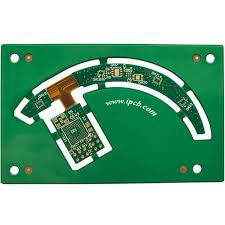
How Does the PCB Board Fabrication Process Work?
Before drilling, the technician looks over each layer to make sure it’s free of any issues that could compromise the integrity of your finished product. This step is important because, as the CM (contract manufacturer) works to turn your PCB design into an actual circuit board, they’ll be relying on your design specifications and layout for information about where each hole goes.
After the drilling is completed, the bare board is ready for its silk-screening, which includes part numbers, symbols, and other information that will be visible on the finished product. Depending on the complexity of your PCB, it may be necessary to use multiple screens in this process to ensure that all of the information is properly transferred.
After silk-screening, the bare board is then ready for the next phase of the PCB fabrication process: solder mask and plating. For the most part, this step is identical for all bare boards, regardless of the number of layers. The only difference is that, for multilayer boards, the solder mask is applied after the etching. This prevents the copper traces from being exposed to the heat of the soldering iron during this phase.
It also protects the underlying metals from corrosion over time. Once the bare board is finished with all of these features, it can then be shipped to the final assembly shop for soldering and finishing. For the best results, your PCB should be designed with ease of manufacturing in mind. This is why it’s important to work with an OEM partner that can provide you with a DRC file or rules file for your PCB design.